


Next: Differential Pair Small Signal
Up: Differential Amplifiers
Previous: Differential Amplifiers
The differential amplifier
is also called the emitter coupled pair,
because,
as shown in figure 5.1,
it has two transistors Q1 and Q2 with their emitters
shorted together.
Figure 5.2:
Differential Amplifier DC Bias
 |
The emitter coupled pair is biased by a DC current source.
In Fig. 5.2, this current source is provided by Q3,
which is a common emitter biasing configuration.
(In contrast to our previous work, the common emitter configuration
of Q3 is not being used as an amplifier, but just to provide a
constant current to the emitter coupled pair.)
Under ideal conditions,
Q3 acts as an ideal DC current source which biases Q1 and Q2.
The transistors
Q1 and Q2
provide the small signal voltage gain, which we will discuss in the next section.
Here, we discuss the DC bias.
We first ground the two inputs.
Now, we provide DC bias by Q3, and
define the DC bias current
sunk by collector Q3 as IEE.
From KCL it is clear that
Then this bias current is split
between Q1 and Q2.
so that
Now, let us assume Q1 and Q2 are identical, then the the DC bias current
IEE is split evenly between them so
| 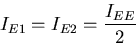 |
(102) |
We now make the excellent approximation that IE1=IC1=IC2.
The DC voltage
at the collectors of Q1 and Q2 is then
If RC1=RC2, then VC1=VC2.
Of course, since the bases of Q1 and Q2 are grounded,
then
| 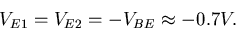 |
(105) |
Just as we did in our other transistor amplifier circuits, for analog
operation, we must ensure that Q1 and Q2 are in the forward active
region of operation. So, when designing our amplifier, we must
make sure that our transistors are not in saturation 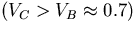 .So, to zero order approximation, we usually choose RC and IC so that
 . This will help you to obtain virtually maximum
swing of your AC signal.
. This will help you to obtain virtually maximum
swing of your AC signal.
Next: Differential Pair Small Signal
Up: Differential Amplifiers
Previous: Differential Amplifiers
Neil Goldsman
10/23/1998