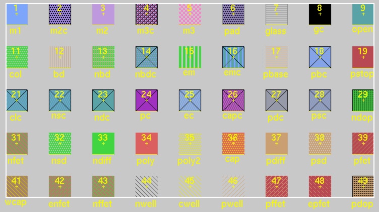
 extended palette for MOSIS SCNA magic layout
 [if downloading it directly (via ftp) then after downloading strip off the .doc suffix (needed to preserve text nature of file)]:
= 3 metal, 2 poly, npn analog SCMOS palette.
     This is a file of 4,893 bytes
extended palette for MOSIS SCNA magic layout
The following is a table giving the meaning of these palette entries.
IC Process Names
for palette_09_06_95.mag
|
c=capac. m=mos n=npn |
main abbreviation |
position in palette row, column / CIF |
alternate names |
Magic color, pages in Technology Manual - 09/08/96 |
Purpose |
|
|
bd |
2,2 / CCD |
bccdiffusion |
p. 15 |
buried diffusion for ccd |
|
c |
cap |
4,6 / CEL+CCE |
capacitor, poly cap, pcap |
p. 10 |
poly2 on poly capacitor |
|
|
capc |
3,6 |
|
|
|
|
n |
clc |
3,1 |
collecttorcontact, colcontact,colc, coc |
p. 14 |
npn collector |
|
|
col |
2,1 |
|
|
|
|
|
cwell |
5,5 /CWC |
|
|
linear capacitor option capacitor well |
|
m |
ec |
3,5 |
electrodecontact, econtact, poly2contact, p2c |
p. 6 |
connect metal 1 to poly2 |
|
|
em |
2,5 |
|
|
|
|
n |
emc |
2,6 |
emittercontact, emitcontact |
p. 14 |
npn emitter |
|
|
enfet |
5,2 |
entransistor |
p. 9 |
direct NMOS using poly |
|
|
epfet |
5,8 |
eptransistor |
p. 9 |
direct PMOS using poly 2 |
|
|
gc |
1,8 |
|
|
|
|
|
glass |
1,7 /COG |
|
dark diagonal stripes, p. 15 |
cuts in overglass |
|
m |
m1 |
1,1 /CMF |
metal1 |
blue, p. 3 |
main metal |
|
m |
m2 |
1,3 /CMS |
metal2 |
purple, p. 3 |
connect to pads |
|
m |
m2c |
1,2 /CVA |
via, m2contact, m2cut, v, via1 |
black waffle, p. 5 |
connect metal 1 to metal 2 |
|
|
m3 |
1,5 /CMT |
metal3 |
|
third metal |
|
|
m3c |
1,4 /CVS |
via2 |
|
contact for m3 |
|
|
nbd |
2,3 |
nbccdiffusion |
p. 15 |
input output nodes for ccd |
|
|
nbdc |
2,4 |
nbccdiffcontact |
p. 15 |
contact for ccd |
|
m |
ndc |
3,3 |
ndcontact, ndiffcut |
p. 7 |
metal1 to ndiffusion contact |
|
m |
ndiff |
4,3 /CAA+CSN |
ndiffusion |
green, p. 4 |
NMOS “channel” |
|
|
ndop |
3,9 |
|
|
|
|
|
nfet |
4,1 |
ntransistor |
p. 8 |
direct NMOS |
|
|
nffet |
5,3 |
nfg, doublentransistor, nfoating-gate, nfloatg, nffet |
p. 9 |
NMOS floating gate |
|
m |
nsc |
3,2 |
nnc, nohmic, nncontact, nsubstratencontact |
p. 7, p. 11 |
metal1 to nsubstratendiff contact; use with nsd for nsubstrate contact |
|
m |
nsd |
4,2 |
nndiff, nnd, nohmic, nsubstrateendiff |
light green stippled holes, p. 4 |
substrate contact or guard rings; use with nsc for nsubstrate contact |
|
m |
nwell |
5,4 /CWN |
|
diagonal green stripes, p. 13 |
PMOS substrates |
|
|
open |
1,9 |
|
|
|
|
m |
pad |
1,6 |
|
diagonal stripes on metal 1 over metal 2, p. 15 |
unprotected pad for external connection |
|
n |
pbase |
2,7 /CBA |
pb |
p. 14 |
npn transistor base = P in nwell |
|
n |
pbc |
2,8 |
pbasecontact, pbcontact |
p. 14 |
npn base contact |
|
m |
pc |
3,4 /CCP |
polycontact, pcontact, polycut |
p. 6 |
poly to metal 1 contact |
|
m |
pdc |
3,7 /CCA |
pdcontact, pdiffcut, |
p.7 |
metal1 to pdiffusion contact |
|
m |
pdiff |
4,7 /CAA+CSP |
pdiffusion |
light brown, p. 4 |
PMOS “channel” |
|
|
pdop |
5,9 |
|
|
|
|
|
pfet |
5,7 |
ptransistor |
p. 8 |
direct PMOS |
|
|
pffet |
4,9 |
pfg, doubleptransistor, pfloating-gate, pfloatg, pffet |
p. 9 |
PMOS floating gate |
|
m |
poly |
4,4 /CPG |
p, polysilicon |
red, p. 3 |
“gates” |
|
c |
poly2 |
4,5 /CEL |
e1, p2, electrode |
yellow cross, p. 3 |
“gates” & “capacitors” |
|
|
|
|
|
|
poly2 contact - uses CCE - see cap |
|
m |
psc |
3,8 |
ppc, ppcontact, pohmig |
p. 7, p. 11 |
metal1 to psubstratepdiff contact; use with psd for psubstrate contact |
|
m |
psd |
4,8 |
ppdiff, ppd, pohmic, psugstratepdiff |
light brown with stipple holes, p. 4 |
substrate contact or guard rings; use with psc for psubstrate contact |
|
|
pstop |
2,9 |
|
|
|
|
m |
pwell |
5,6 /CWP |
|
diagonal brown stripes, p. 13 |
NMOS substrates |
|
|
wcap |
5,1 |
|
|
|