ENEE 206
April 13, 2004
Laboratory 15 - Transient Response In 1st and 2nd Order Circuits
A. Lab Goals
In this lab you will design, construct, and test a number of circuits with one or two energy storing elements. The goal of the lab is to characterize and understand the transient response of these circuits.
B. Background Reading
Review the material in (M/L) on first and second order circuits in sections 7.1 - 7.3. Also read about PSpice simulations (with old version) in section 7.7 of M/L.
C. Definitions
- Overshoot - the maximum amount a signal (usually a voltage) exceeds its steady state value as the circuit transitions to equilibrium. For example, if the maximum voltage is Vm and the steady-state voltage is V0, the percentage overshoot is:
OS = (Vm/V0 - 1) * 100%.
- Ringing - the oscillation phenonena that occurs in an underdamped circuit as it approaches equilibrium.
D. Laboratory Equipment
The LC meter and DMMs will be used to measure component values. Transient responses will be recorded by using the oscilloscopes in single-shot mode.
E. New Hardware
No new hardware is used in this lab.
F. Circuit Analysis
In this section we are going to briefly REVIEW the transient response for several simple circuits. We are always going to use the transfer function approach to solve tor the homogeneous solutions and will leave everything in complex frequency notations: s = jw ~ d/dt.
 The first circuit we will analyze is the RL series combination shown in Fig. 15.1. KVL for t > 0 yields
5 = L(di/dt) + Ri(t) [ -> 5 = (Ls + R)I]
Thus, the particular solution is
ip = 5/R
and the homogeneous solution is
ih(t) = i0e-Rt/L
The initial condition i0 is found from the total solution i(t) = ih + ip(t), after using the continuity of inductor current principle and the fact that the switch is open for t < 0. The final answer is
i(t) = (5/R)(1 - e-Rt/L).
The corresponding voltage across the resistor is plotted in Fig. 15.2. How could we determine the inductances L without an LC meter?
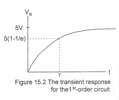
 We know the starting and ending values of the resistor voltage, so we can pick a point in between, measure the voltage at that time and choose L so that the above equation agrees. For example, if we pick the point where the voltage has achieved (1 - e-1) = 63.2% of its final value, the time t that the voltage occurs can be used to find L (assuming a DMM was used to get R):
L = Rt.
The second circuit we'll analyze is the RC series circuit shown in Fig. 15.3a. It may be more convenient to convert the nonideal voltage source to a nonideal current source and solve the KCL problem (see Fig. 15.3b):
5/R = vc/R + Cdvc/dt ( -> 5/R = (1/R + sC)VC)
So the particuular solution is
vp(t) = 5 V
and the homogeneous solution is
vh(t) = V0e-t/RC.
Using the principle of continuity of voltage across capacitors, and the "fact" that the capacitor voltage is zero when the switch is open, we arrive at
vc(t) = 5(1 - e-t/RC)V.
This solution is not plotted because it is identical in form to the resistor voltage plotted in Fig. 15.2. The only difference is in the time constant which is t = RC for this circuit and t = L/R for the previous case. How could we derermin C from oscilloscope data?
We know the starting and ending values of the resistor voltage, so we can pick a point in between, measure the voltage at that time and choose L so that the above equation agrees. For example, if we pick the point where the voltage has achieved (1 - e-1) = 63.2% of its final value, the time t that the voltage occurs can be used to find L (assuming a DMM was used to get R):
L = Rt.
The second circuit we'll analyze is the RC series circuit shown in Fig. 15.3a. It may be more convenient to convert the nonideal voltage source to a nonideal current source and solve the KCL problem (see Fig. 15.3b):
5/R = vc/R + Cdvc/dt ( -> 5/R = (1/R + sC)VC)
So the particuular solution is
vp(t) = 5 V
and the homogeneous solution is
vh(t) = V0e-t/RC.
Using the principle of continuity of voltage across capacitors, and the "fact" that the capacitor voltage is zero when the switch is open, we arrive at
vc(t) = 5(1 - e-t/RC)V.
This solution is not plotted because it is identical in form to the resistor voltage plotted in Fig. 15.2. The only difference is in the time constant which is t = RC for this circuit and t = L/R for the previous case. How could we derermin C from oscilloscope data?
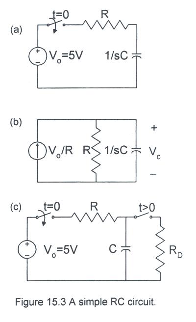 Let's be a little careful about this "fact" of zero initial voltage. When the switch is open, there is no discharge path for the capacitor, so it may well be charged. When performing the experiment, it is best to have a second switch that places a discharge resistor in parallel with the capacitor (as in Fig. 15.3c).
Now consider the RLC series circuit shown in Fig. 15.4.
 The current through the passive components is:
V0 = Ri + Ldi/dt + (1/C)Sidt [ -> V0 = (R + sL + 1/sC)I.]
It's more convenient to write this in terms of the capacitor voltage:
i = C(dvc/dt) => Vc = I/sC.
Combining this last expression with the KVL equation yields:
V0 = LCd2vc/dt2 + RCdvc/dt + vc ( -> V0 = (s2LC + sRC + 1)Vc. )
Thus, the particular solution is
vp = 5V.
There are three possible homogeneous solutions depending on the sign of the discriminant
D = (R/2L)2 - 1/LC.
If D = 0, R = 2(L/C)1/2 and the circuit is critically damped, so the homogeneous solution is:
vh = Ae -st + Bte -st for s = R/2L
The initital condition for the inductor is i = 0, and this implies that dVc/dt = 0, but the capacitor voltage may not be discharged unless a discharge resistor is used as in Fig. 15.3c. If Vc(0+) = 0, then
vc(t) = 5[1 - e -st(1 + st)]V
However, if R > 2(L/C)1/2, D > 0, the system is overdamped and vh = Ae s1t + Be s2t for
s1,2 = -R/2L +/- [(R/2L)2 - 1/LC]1/2.
Finally, if R < 2(L/C)1/2, D < 0, the system is underdamped and
vh(t) = e -st[Acos(wt) + Bsin(wt)]
for
w = [1/LC - (R/2L)2]1/2.
In the lab you are supposed to design one circuit of each type. It's probably easiest to pick one inductor and one capacitor that are convenient, then choose three resistors: one that's matched, one smaller, and one larger.
The current through the passive components is:
V0 = Ri + Ldi/dt + (1/C)Sidt [ -> V0 = (R + sL + 1/sC)I.]
It's more convenient to write this in terms of the capacitor voltage:
i = C(dvc/dt) => Vc = I/sC.
Combining this last expression with the KVL equation yields:
V0 = LCd2vc/dt2 + RCdvc/dt + vc ( -> V0 = (s2LC + sRC + 1)Vc. )
Thus, the particular solution is
vp = 5V.
There are three possible homogeneous solutions depending on the sign of the discriminant
D = (R/2L)2 - 1/LC.
If D = 0, R = 2(L/C)1/2 and the circuit is critically damped, so the homogeneous solution is:
vh = Ae -st + Bte -st for s = R/2L
The initital condition for the inductor is i = 0, and this implies that dVc/dt = 0, but the capacitor voltage may not be discharged unless a discharge resistor is used as in Fig. 15.3c. If Vc(0+) = 0, then
vc(t) = 5[1 - e -st(1 + st)]V
However, if R > 2(L/C)1/2, D > 0, the system is overdamped and vh = Ae s1t + Be s2t for
s1,2 = -R/2L +/- [(R/2L)2 - 1/LC]1/2.
Finally, if R < 2(L/C)1/2, D < 0, the system is underdamped and
vh(t) = e -st[Acos(wt) + Bsin(wt)]
for
w = [1/LC - (R/2L)2]1/2.
In the lab you are supposed to design one circuit of each type. It's probably easiest to pick one inductor and one capacitor that are convenient, then choose three resistors: one that's matched, one smaller, and one larger.
PSpice simulation


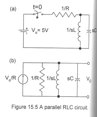
Now consider the parallel RLC circuit shown in Fig. 15.5a. After transforming the battery to a nonideal current source as in Fig. 15.5b we can use KCL to get
V0/R = vc/R + (1/L)Svcdt + Cdvc/dt -> [V0/R = (1/R + 1/sL + sC)Vc.),
It's actually easier to solve for iL(t):
Vc = VL = sLIL
IL = V0/(s2LCR + sL + R).
So the particular solution is
ip(t) = V0/R = 5/R (Amps),
and the homogeneous roots are
s1,2 = -1/2RC +/- [(1/2RC)2 - 1/LC]1/2]
There are three different types of solutions corresponding to critically damped, underdamped, and overdamped cases. The forms are the same as the forms shown for the RLC seies case and are not repeated here. The dividing line between the three cases is different, however. For the RLC parallel case, the circuit is critically damped when
R = (1/2)(L/C)1/2.
Furthermore, the circuit is underdamped whenever R > (1/2)(L/C)1/2 and overdamped whnever R < (1/2)(L/C)1/2. For RLC series circuit, the solution was underdamped if the resistance was too low. In contrast, the RLC parallel circuit is underdamped if the resistance is too high, Can you explain the difference between the two cases?
With the oscilloscope, we will measure the voltage across the LC circuit and not the current, so we must use the terminal relationshiop between the inductor voltage and current. Let's look at the ciritically damped case as a specifid example. Now the initial conditions are zero current through the inductor and zero voltage across the capacitor (no damping rsistor is required - do you know why?) Thus, the total current through the inductor is:
iL(t) = (5/R)[1 - (1 + st)e -st] for s = 1/(2RC).
The inductor (and therfore capacitor) voltage is
vL(t) = LdiL/dt = 5(L/R)s2te-st = (5/RC)te-t/2RC V.
Note that the voltage approaches zero as time goes to infinity. The maximum voltage can be found by setting the voltage derivative to zsro:
Vmax = 10e-1 ~ 3.68 (V)
at
tmax = 2RC.
Note that the voltage maximum is independent of R and L. Also note that if the oscilloscope trigger is set above 3.68 V, the scope will never trigger when you pulse the circuit!
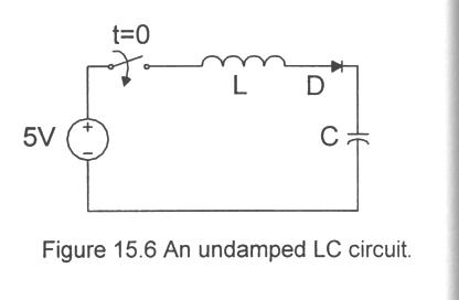 An example of an undamped LC series circuit is shown in Fig. 15.6. The reason for the diode will become evident later. Since the diode will be "on" while the capacitor is charging, we can just replace it with a switch for now. We have already done the analysis, since it is the same as the RLC series circuit with R = 0. The solution, taking into account zero initial capacitor voltage,is the solution is:
vc(t) = 5[1 - cos(wt)] (V)
for w = 1/(LC)1/2.
An example of an undamped LC series circuit is shown in Fig. 15.6. The reason for the diode will become evident later. Since the diode will be "on" while the capacitor is charging, we can just replace it with a switch for now. We have already done the analysis, since it is the same as the RLC series circuit with R = 0. The solution, taking into account zero initial capacitor voltage,is the solution is:
vc(t) = 5[1 - cos(wt)] (V)
for w = 1/(LC)1/2.
The current through the capacitor is:
ic(t) = C(dvc/dt) = 5(L/C)1/2sin(wt)A.
The current becomes zero when wt = t/(LC)1/2 = p or t = p(LC)1/2.
At that point the diode turrns off and the voltage on the capacitor stays constant. The maximum capacitor voltage is vc(p(LC)1/2)) = 5(1 - cosp) = 10V. Thus, this circuit, known as a resonant charging circuit, charges the capacitor up to twice the battery voltage!
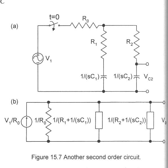 As a final example, consider the two capacitor circuit shown in Fig. 15.7a. The transformation shown in Fig. 15.7b aids in the analysis of the circuit. The transfer function of the output voltage Vc2 to the input voltage V1 can be shown to be:
Vc2/V1 = (sR1C1 + 1)/[s2C1C2(R0R1 + R0R2 + R1R2) + s(C2R0 + C1R0 + C1R1 + C2R2) + 1]
The initial conditions, homogeneous solution, etc., can all be found by applying the principles you learned in ENEE 204. [see section 7.4 in (M/L)]
As a final example, consider the two capacitor circuit shown in Fig. 15.7a. The transformation shown in Fig. 15.7b aids in the analysis of the circuit. The transfer function of the output voltage Vc2 to the input voltage V1 can be shown to be:
Vc2/V1 = (sR1C1 + 1)/[s2C1C2(R0R1 + R0R2 + R1R2) + s(C2R0 + C1R0 + C1R1 + C2R2) + 1]
The initial conditions, homogeneous solution, etc., can all be found by applying the principles you learned in ENEE 204. [see section 7.4 in (M/L)]
Helpful Hints
- Make certain that you discharge the capacitors in all series RC & RLC circuits.
- Recall that you will be using the oscilloscope in single-shot mode. The autoscale button eill not be of any use and you will need to select the trigger parameters carefully.
- Remember to discharge capacitors between "shots" in any circuit that doesn;t naturally have a discharge path for the capacitor (e.g. series circuits).
- Switch bouncing, which you learned about during some of the digital labs, can also cause a problems. If ...
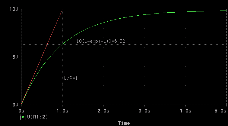
- To help with the PSpice simulations (with old version) of the transient circuits, you can download a PSpice example called "lab15.sch". The example has an RC circuit that is deiven lby a 5V battery which is connected to the circuit by a switch (sw_tClose) that closes ar t = 0. The capacitor is shortyed for t < 0 by a 1 W resistor that is disconnected by a switch(sw_tOpen) at t = 0. This is not really necessary for the simulation, but you may nmeed to discharge capacitors between successive attempt during the lab. The simulation is set up to do a transient analysis. Take a careful look at the setup menus to see how this analysis shoud be run. Additional information can be found in the 204 book and in the PSpice references. If when you click on the link you see a text file, you can copy the text file and save it on your computer as "lab15.sch", or you can go back and click on the link with the rigfht mouse button and select "save link as" from the menu.
Laboratory 15 Description - Transient Response in 1st and 2nd-Order Circuits
Objective:
To characterize transient signals in circuits with energy-storing elements.
Available Hardware:
Analog boxes - see Appendix G and DIP-swtche or momentary switches.
Inductors: 4.7 mH, 10 mH, 20 mH, 50 mH
Do lab 15x from the table below, where the letter x corresponds to your group. (Note that this table is different from that in the lab manual.)
| Lab | R1 | R2 | C1 | C2 | C3
|
|---|
| 15a | 51 W | 220 W
| 4.7 mF | 22 mF
| 220 mF
|
|---|
| 15b | 220 W | 470 W
| 100 nF | 22 mF | 220 mF
|
|---|
| 15c | 470 W | 1 kW
| 100 nF | 1.0 mF | 220 mF
|
|---|
| 15d | 1 kW | 2 kW
| 100 nF | 1.0 mF | 4.7 mF
|
|---|
| 15e | 33 W | 220 W
| 470 pF | 1.8 nF | 10 mF
|
|---|
| 15f | 3.3 kW | 4.7 kW
| 68 nF | 3.3 mF | 22 mF
|
|---|
Pre-lab preparation
Part I - First-order circuits
- Draw the wiring diagram for a switched RL circuit powered by a 5 V battery.
- Draw wiring diagrams for a switched RC circuit poweered by a 5 V battery.
- Simulate the circuit in the previous step for R1 and C1. Plot the voltage across the capacitor as a function of time.
Part II - Second-order RLC circuits
- Draw the wiring diagram for a switched RLC circuit powered by a 5V battery. Given the available components, find RLC combinations that are overdamped, underdampped, and critically-damped (1 each).
- Simulate the circuit in the previous step for the underdamped case. Plot the voltage across the capacitor as a function of time.
- Draw the wiring diagram for a switched LC parallel circuit with a series resistance R) powered by a 5 V battery. Given the available components find an RLC combination that is neaerly critically-damped.
- Simulate the circuit in the previous step. Plot the voltae across the the capacitor as a function of time.
that is nearly critically damped.
Part III - Second-order two-capacitor circuits
- simulate the circuit shown in Fig. 15.8(a) for V1 = 5cos(12pt). Plot the voltages across C1 and C2 as a function of time. Be certain that initial conditions are correct. What is the maximum voltage on eaxch capacitor and what is the peak voltage in steady-state (on each capaciror)?
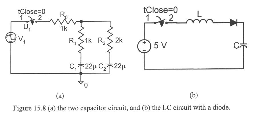
Part IV - Resonant charging circuit
- Simulate the circuit in Fig. 15.8(b) assuming that L = 50 mH, C = 22 mF, and the Quality factor (Q) of the inductor is 5 at the circuit's resonant frequency. Plot the voltage on the capacitor as a function of time. Short the diode and repeat the simulation and plot.
Experimental Procedure:
During this experiment, be certain that you:
- Ask the TA questions regarding any procedures about which you are uncertain.
- Turn off all power supplies any time that you make any change to the circuit.
- Arrange your circuit components neatly and in a logical order.
- Compare your breadboards carefully with your circuit diagrams before applying power to the circuit.
- Complete the following tasks:
Part I - Preliminary measurements
- Measure the dc resistances of all resistors and inductors to be used in the circuits.
- Measure the inductances and capacitances with the LC meter.
Part II - First-order circuits
- Construct the switched RL circuit with a 51 W resistor and the 4.7 mH inductor.
- Operate the oscilloscope in triggered mode and plot the voltage across the resistor as a function of time.
- Measure the time constant for the circuit.
- Repeat the previous measurement with the 10 mH, 20 mH and 50 mH incuctors (but do not make additional plots).
- Construct the switched RC circuit with a R2 resistor and the C1 capacitor.
- Plot the voltage across the capacitor as a function of time.
- Measure the time condtant for the circuit.
- Repeat the prevoius measurement with the C2 and C3 capacitors (but don't make more plots).
Part III - Second-order RLC circuits
- Construct the switched RLC series circuit with the values you selected for the underdamped circuit.
- Plot the voltage across the capacitor with time. (Make sure that you choose a time interval greater than the period of the oscillation so that hyou can attempt to measure the oscillation frequency.)
- Repeat the above plot for the overdamped and critically-damped circuits.
- Construct the switched RLC parallel circuit.
- Plot the voltage across the capacitor with time.
Part IV - Second-order two-capacitor circuit
-
-
-
Part V - Resonant-charge circuit
-
-
-
Post-lab analysis:
Generate a lab report following the sample report available in Appendix A. Mention any difficulties encountered during the lab. Describe any results that were unexpected and try to account for the origin of these results(i.e. explain what happened). In ADDITION, answer the following questions/instructions:
Part II - First-order circuits
-
Part III - Second-order RLC circuits
-
-
-
-
-
Part IV - Second-order two-capacitor circuit
Part V - Resonant-charge circuit
-
-
